In a 1,000-level clean room at 3 a.m., a 12-inch wafer worth $30,000 is sliding toward the photolithography machine. Suddenly, a slight tremor in the robotic arm deflects the wafer by 0.5 microns - the equivalent of a foot slipping 1 centimetre while shooting a goal on a football pitch. The result? The entire batch of chips was scrapped, costing over a million dollars. Such a tragedy is being ended by magnetic levitation technology.
Photolithography Battlefield: Magnetic Levitation Lifts Nanoscale Precision
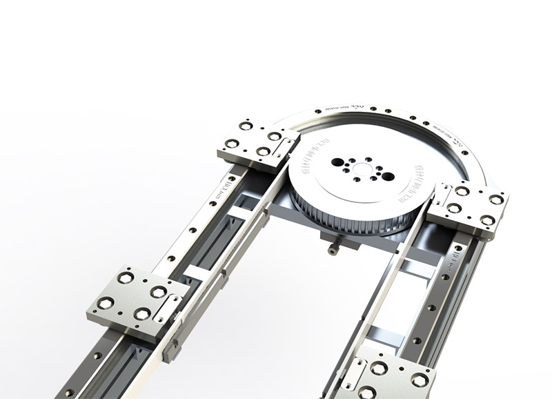
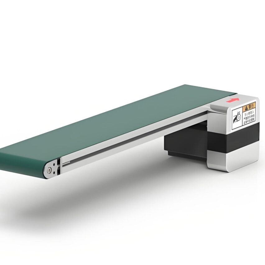
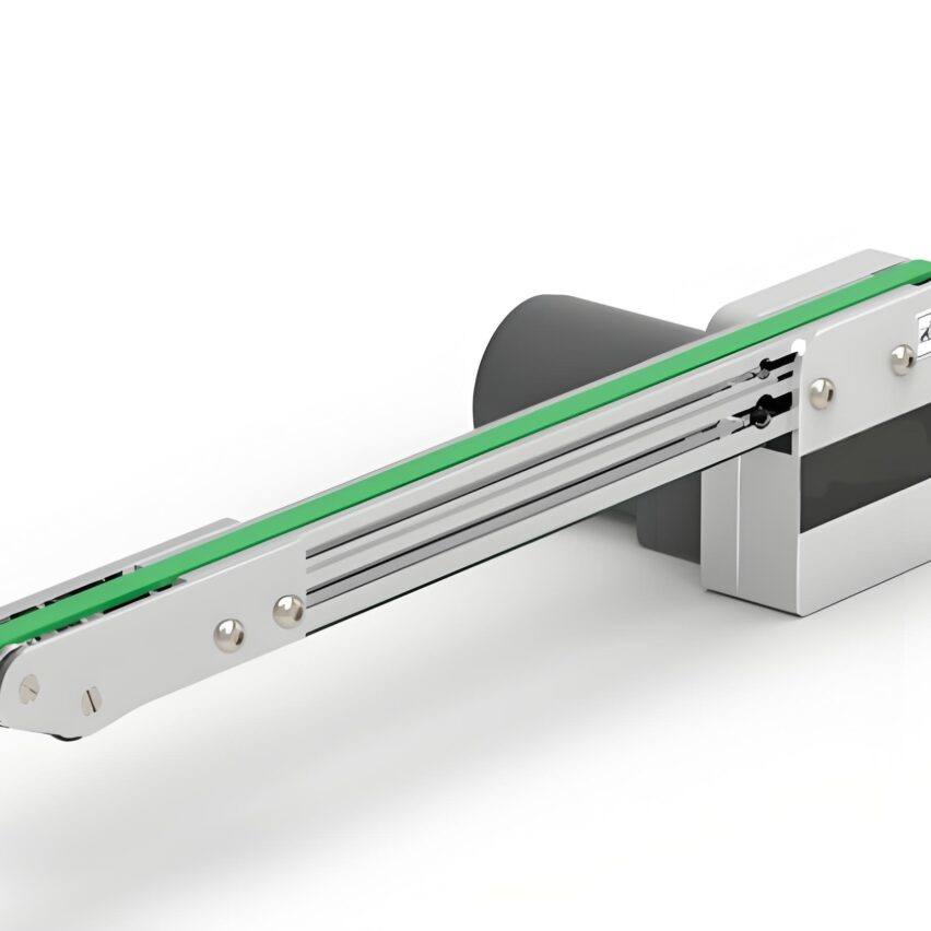
As the wafer enters the lithography machine, the magnetically levitated dual workpiece table is quietly activated:
- Nanoscale stabilisation: The magnetic levitation platform forms a stable magnetic field through an array of more than 2,200 permanent magnets (precision ±20 microns), controlling vibration to within 0.1 nanometres. Compared with the traditional air-floating platform, the positioning accuracy is improved by 10 times.
- double stage ballet: The exposure stage is moving at 5m/s while the measurement stage calibrates the next wafer. Magnetic levitation allows seamless switching between the two tables, increasing efficiency by 30%
- Vacuum Environment Breakout: EUV lithography requires a vacuum environment where conventional air float fails. The stability of the magnetic levitation platform in vacuum has enabled sub-7nm chip yields to soar from 70% to 92%.
A memory chip factory measured: the introduction of magnetic levitation workpiece table, lithography alignment error from ± 1.2nm down to ± 0.3nm, equivalent to the deviation in the hair engraved on the word reduced to one ten thousandth.
Etching Session: Precision Engraving under Multiple Magnetic Fields
The moment the door of the etching machine opens, the magnetic levitation technology shows its power again:
Scenario 1: The Plasma Control Revolution
Wuxi Suncorp's Multi-field Etcher is in action:
make a copy of[permanent magnet array] → [constrained first magnetic field] → [excited plasma] [electromagnetic coils] → [enhanced second magnetic field] → [accelerated ion bombardment]This design allows a plasma density increase of 401 TP3T, an etch rate increase of 351 TP3T, and a wafer edge uniformity deviation of <21 TP3T.
Scenario 2: Zero Vibration Transmission
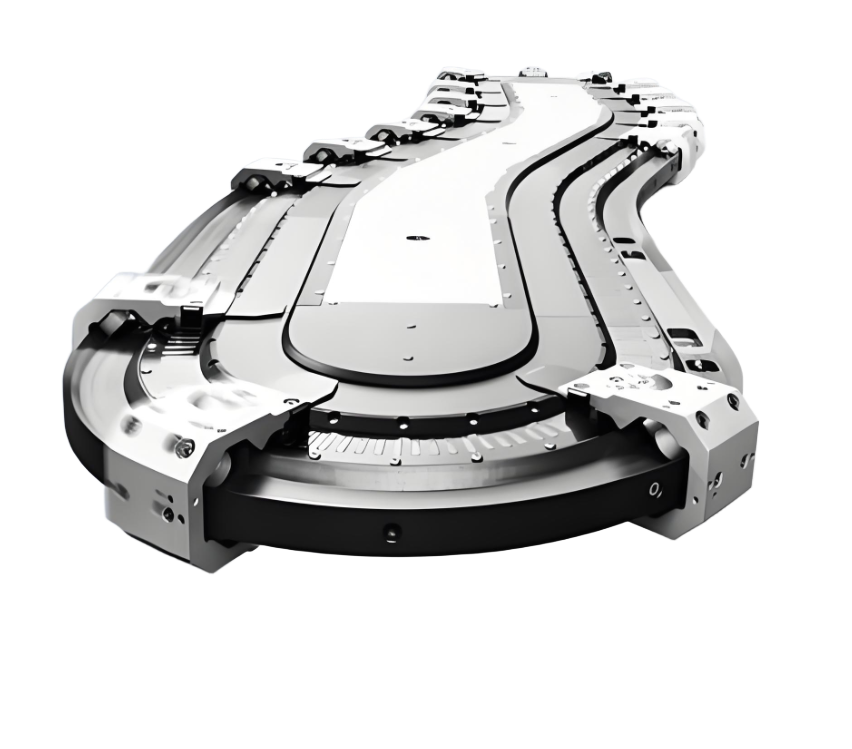
The etched wafer requires millisecond transit:
- Magnetically levitated kinetochore carts carrying wafers gliding along a track at 4m/s
- Acceleration up to 1.5G during emergency stop, but vibration amplitude 10μm)
- A 3D NAND production line validation: silicon through-hole (TSV) etch depth consistency improvement of 22%
Full Process Handling: A Dust-Free Network Woven by Magnetic Levitation
From photolithography to etching, the wafer travels through a 200-metre clean corridor:
| annular ring | Traditional approach pain points | Magnetic Levitation Solutions |
|---|---|---|
| Cross-equipment transfer | Metal dust generated by robots | Vacuum Magnetic Levitation Pipeline Confined Conveying |
| Process Station Docking | Positioning error ±0.1mm | Laser positioning ±0.01mm precise docking |
| emergency rework | Manual handling leads to a breakage rate of 3% | Intelligent actuator air rerouting, 0 contact |
Fruit Chestnut's iHS system also realises an "air logistics network": 200+ motors are dispatched by AI, weaving invisible tracks in the semiconductor workshop. When an etching machine breaks down, the wafers can automatically switch routes within 0.5 seconds and run to the backup equipment.
Domestic breakthrough: from catching up to defining standards
Once upon a time, the magnetic levitation wafer table was monopolised by ASML. Now the battlefield is reversed:
- Precision benchmarking: Shanghai Microelectronics Magnetic Levitation Turntable Reaches ±0.1μm, Compares to ASML NXT Series
- Costs cut in half: Domestic kinematic trolley unit price reduced from $80,000 to $30,000, maintenance response reduced from 2 weeks to 24 hours
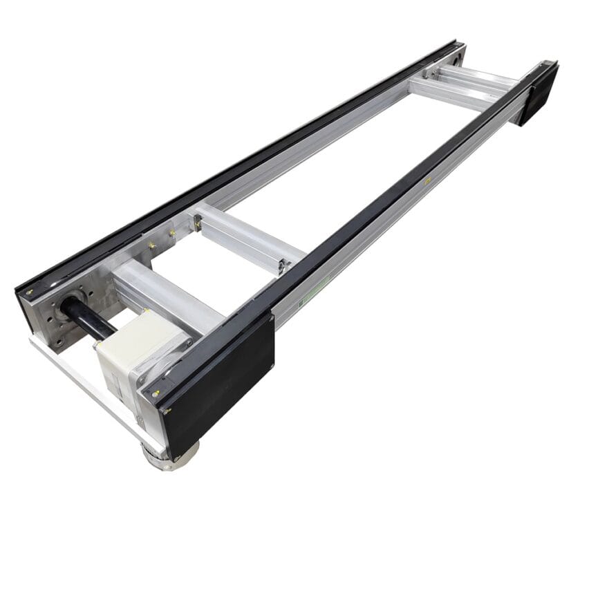
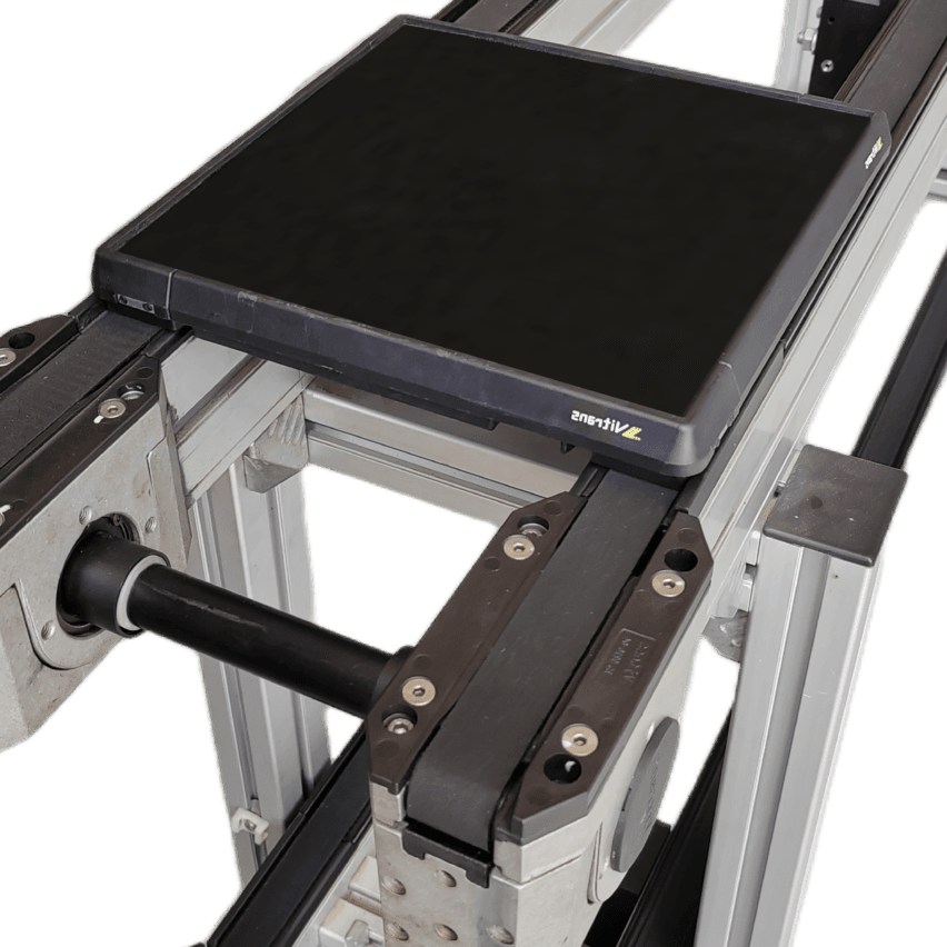
- Scenario Innovation: Nanjing XunTrans Technology combines magnetic levitation and AI to realise in the post-etching inspection session:
make a copy of[Wafer Scanning] → [AI Identifies Defects] → [Magnetically Levitated Needle Precision Repair]Keeps rework costs down 60%
Industry data show that: 2025 domestic maglev equipment in lithography / etching link penetration rate exceeded 45%, every 10 pieces of high-end chips in the world, there are 4 pieces of Chinese maglev system polished.
The core logic of this silent revolution is very straightforward - when the chip circuit is as fine as 3 nanometres, any particle of dust, a hint of vibration is a fatal killer. And magnetic levitation with "no contact" wisdom, is the chip war in the hinterland erected a new technology moat.